Open as PDF
 With the ever increasing demand for higher data rates and lower power consumption, power and signal integrity are playing a larger role in the design of modern electronic devices. Demand from industry and consumers for higher throughput, more bandwidth and longer battery life mean stricter requirements and tighter tolerances on semiconductor and device design, test and manufacturing. These emerging challenges cannot be addressed through simulation alone, driving the need for real world evaluation and tolerance testing.
For over 30 years Noisecom has been designing noise generation devices and instruments for Carrier-to-Noise, jamming, multipath fading, satellite test and calibration across a wide variety of industries. Noisecom has a depth of experience unmatched in the industry and works closely with technical end users to find the right product for their application with both off the shelf and customized solutions. This experience and close links to customers and markets has led to the development of noise generators specifically designed for high speed data applications where real world power and signal integrity challenges exist.
Semiconductor device designers must ensure that their components operate properly at high data rates when integrated into a real world system. Design or fabrication issues can cause jitter, impacting chip and system functionality, and leading to increased bit error rate. Testing for these types of signal integrity issues requires the use of real world interfering signals to test the system tolerance for jitter and crosstalk. Noisecom J7000 and J9000 jitter generators add broadband noise to the data lines to stress test system performance. Jitter can be added to single-ended or differential channels in frequency ranges from 1 MHz to 13 GHz.
Designers developing systems that integrate high speed semiconductors must ensure that these components can be powered correctly and function at high data rates. Modern system performance requires lower supply voltages which are often impacted greatly by interference or system noise from power supply lines, noisy clocks or data coupling on to the lines. These power integrity challenges must be tested before new products can be deployed. Noisecom JV9000 noise generators add interfering noise and CW impairments to a voltage supply which is then applied to the device under test to test device tolerance to noisy supply lines found in the real world. Noise generation is available in a variety of voltage and current configurations across a range of different frequencies.
 Customization
Each device is different and the set of power and signal integrity challenges and requirements can vary from device to device and system to system. This diverse range of unique testing requirements is why Noisecom jitter and noise solutions are highly customizable. Jitter and noise generators can be designed for different noise power density, internal filtering, remote control, and differential signaling. Whether it is small modifications to requency or voltage output or a fully custom solution, Noisecom has a broad range of capabilities and solutions for every budget.
Power Integrity – Noise on Vcc and Power Supply Rejection Ratio
New semiconductor devices are being driven by lower supply voltage levels resulting in noise on voltage rails (Vcc) becoming a critical issue driving system performance. With increased internal density of chipsets, closer spacing of traces on PC boards, and growing board layer count, noise and interference is more easily coupled on to other paths including the Vcc line. External and internal interference can couple onto data and voltage lines resulting in jitter on clock signals or noise on amplifier outputs leading to an increase in bit error rate and a decrease in system performance.
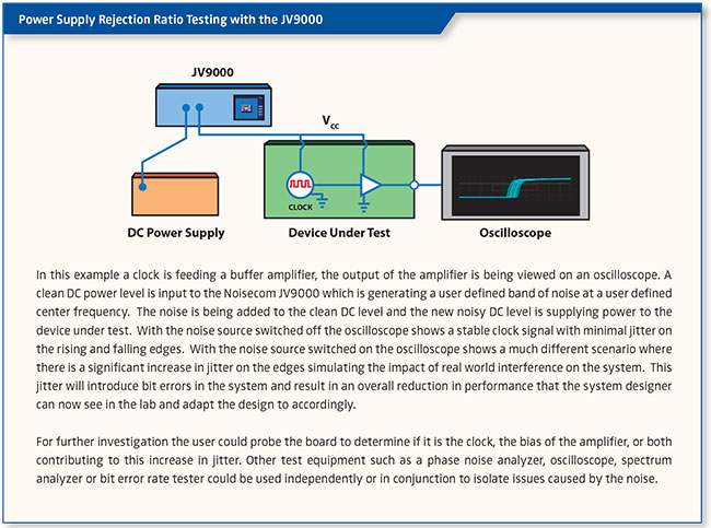
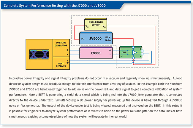
Noisecom JV9000 instruments allow system designers to stress chipsets by adding controlled levels of broadband noise or CW interferers on to a clean power supply. The output from the noise generator is applied directly to the device under test enabling a test of the device under real-world conditions simulating a noisy environment. The internal signal generator can sweep frequencies and change power levels to see how the device responds and reacts to a wide variety of noise and interfering signals. When used in conjunction with other equipment such as an oscilloscope and a bit error rate tester engineers can analyze system performance and then quantify and qualify how much noise on voltage rails or inputs to the device the system can tolerate. This controlled environment allows engineers to specify this performance and tolerances in a datasheet. Further capabilities of a JV9000 allow for determination of resonant frequency of a device by sweeping the internal signal generator. At resonance the majority of the signal will disrupt the output of the device and systems designed with this device can be built accordingly.
Signal Integrity - Jitter and Crosstalk
High speed semiconductor devices and serial data communications links are being pushed to faster and faster speeds while being forced to small form factors with tight spacing. As speeds increase the challenges of maintaining a minimum bit error increase as emerging next generation standards are built upon faster rise times, multi-level signaling methods, increased symbol speeds and tighter jitter tolerances. Shrinking form factors mean noisy components and potential sources of crosstalk are located nearby the communications link. Spacing of traces, noise from power supplies, or interference from crosstalk aggressors like a nearby clock or additional data lines all can add jitter to a communications link, resulting in increased bit error rate, deviation from the specification and reduction in system performance.
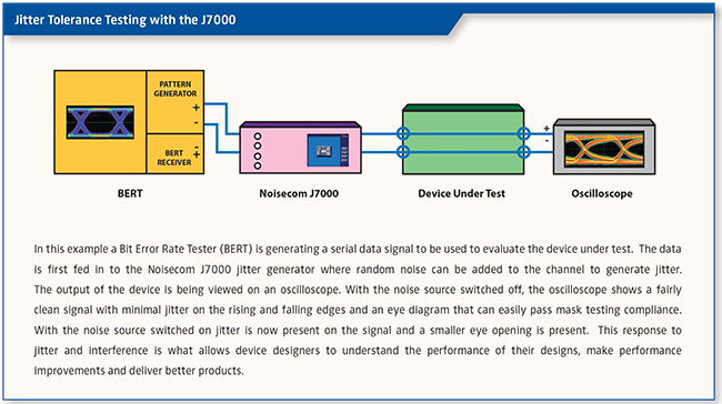
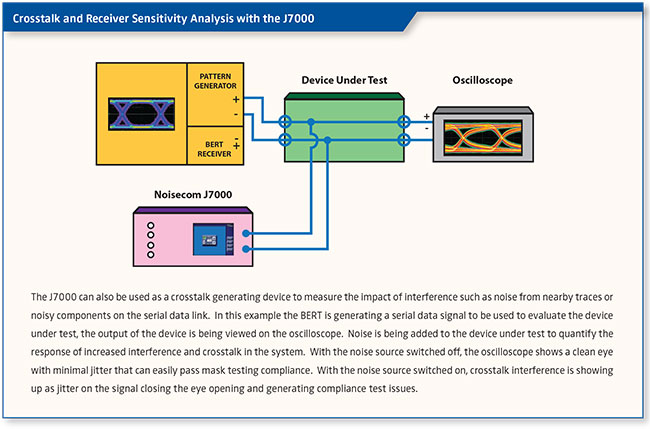
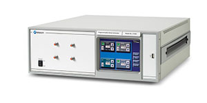 Design simulation allows device and system engineers to identify potential issues before releasing their designs, however in the lab or final system when the device needs to be incorporated into a real-world system additional sources of interference will exist. The Noisecom J7000 and J9000 noise and jitter generators enable testing of designs as they move from simulation to fabrication giving design and test engineers the ability to quantify and qualify how their device responds to sources of interference in the final system. The J7000 and J9000 instruments are capable of generating high crest factor, precise controlled interference that can be injected to a circuit or device to create random jitter. This type of interference is ideal for testing devices built for next generation PCI Express, Serial ATA and Fiber Channel standards as well as emerging signaling methods like PAM4. The truly random nature of the noise generators are designed to model real world electrical noise commonly found in high speed serial data communications links. The noise is user controllable for signal-to-noise and the signal path has a nominal insertion gain of 0 dB, with very low amplitude and phase ripple. Fully customizable jitter generators can be developed for multiple channels, single-ended and differntial data and a variety of filtering.
J7000 Jitter Noise Generator
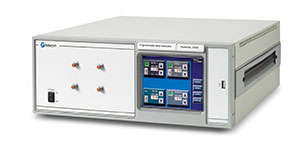 The J7000 series has 6 standard models, but custom frequencies, power, and flatness specifications can be provided. This instrument has up to five optional bandlimiting filters that can be added for specific serial data applications. Differencial inputs and outputs are available in the J9000 series.
Features and Benefits
- Serial Data sources and specialized filters available (consult factory)
- Provides > 18 dB crest factor ( +/- 7σ)
- 127 dB attenuation in 1 dB, or optional 0.1 dB steps
- Units > 2 GHz have 79.9 dB total attenuation
- Summing input for CNR, or Eb/No measurements
- Standard Ethernet, or optional GPIB remote control
- Optional rear panel connectors
| J7000A Series |
Output Characteristics |
| Model |
Frequency Band |
Power (dBm) |
Vrms |
dBm/Hz |
Flatness (dB) |
| J7105A |
1 MHz - 10 MHz |
-3 |
0.16 |
-73 |
±0.25 / 40 MHZ |
| J7107A |
10 MHz - 100 MHz |
-3 |
0.16 |
-83 |
±0.25 / 40 MHZ |
| J7108A |
10 MHz - 500 MHz |
-3 |
0.16 |
-90 |
±0.25 / 40 MHZ |
| J7109A |
10 MHz - 1 GHz |
-3 |
0.16 |
-93 |
±0.25 / 40 MHZ |
| J7112A |
10 MHz - 2 GHz |
-3 |
0.16 |
-96 |
±0.25 / 40 MHZ |
| J7115A |
10MHz - 5 GHz |
-3 |
0.16 |
-100 |
±2.5 dB |
| J7113A |
1 GHz - 13 GHz |
-3 |
0.16 |
-107 |
±3 dB |
| Specifications |
|
| Output noise power |
-3 dBm (+/- 0.5 dBm) |
| Output noise band |
up to 32 GHz |
| Noise attenuation |
0 to 63 dB in 0.1 dB steps |
| Noise attenuator |
±0.2 dB or 0.5% |
| Signal path gain |
0 ±1 dB |
| Standard connectors |
SMA female |
| Power |
115 VAC, 60 Hz |
| Operating Temperature: |
-10° to +65°C |
| 6.25” color VGA, TFT touch screen |
|
| Ultra-low distortion signal path |
|
JV9000 Specifications
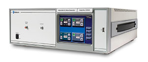 The JV9000 Adjustable Vcc Noise Generator is designed to test components that need to be qualified for immunity to specific interference levels. The instrument has the capability to inject noise and deterministic jitter (Dj) signals into Vcc lines. JV9000 is a very useful instrument to analyze Power Supply Rejection Ratio.
Features and Benefits:
- Noise Generator (white Gaussian noise): 500 Hz to 2 GHz, 0dBm
- CW/Spur Generator: up to 3 GHz (optional)
- Higher input current options
- Customized inputs, outputs and signal levels possible
- All computerized versions and remote programmable
| Input |
| Maximum Voltage |
5V |
| Maximum Current |
500 mA, higher options available (opt23 and opt24) |
| Connector |
BNC (F) |
| Noise Source (white Gaussian noise) |
| Impedance |
50 Ohms SMA, optional BNC (F) - (opt01) |
| Frequency Range |
1 kHz to 500 MHz (500 Hz - 2 GHz operational), custom frequency (opt09) |
| Output Power |
0 dBm min. (at the output of bias-T), adjustable 127 dB, 0.1dB step into 50 Ohms
Higher power (+10 dBm - opt05) |
| CW/Spur Generator (optional) |
| Impedance |
50 Ohms (typ.) |
| Frequency Range Options |
1 kHz to 25 MHz (opt21), programmable, 100 Hz resolution or 1 Hz resolution (opt06)
25 MHz to 3 GHz (opt22), programmable, 100 kHz resolution or 1 kHz resolution (opt07) |
| Output Power |
0 dBm min. (at the output of bias-T), adjustable, 127 dB, 0.1 dB step, into 50 Ohms,
harmonics 20 dBc or less (40 dBc for discrete tones optional)
Higher power (+10 dBm - opt05) |
| Auxiliary Input (opt08-x) |
| Input Frequency Range |
1 KHz - 3 GHz |
| Maximum Input Power |
+10 dBm |
| Auxiliary Input Connector |
50 Ohm SMA, optional BNC (opt01) |
| Level Control |
adjustable, 127 dB, 0.1 dB step |